Monday, August 30, 2010

Mini UPS System Circuit

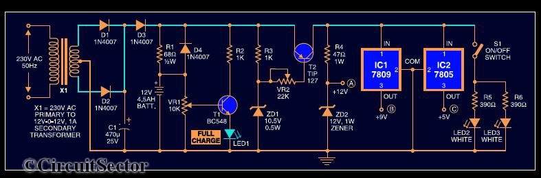
Here's the circuit diagram of a mini low power UPS system which provides uninterrupted power supply to operate dc powered instruments of voltage rating 12V, 9V and 5V up to 1A current. The takes the load from mains without any spikes or considerable delay. The circuit involves the over charge and deep discharge of the battery for long life.

Mini UPS circuit working

Circuit Diagram of Mini UPS System : Click  to enlarge

The UPS system consist of a 12-012 standard stepdown transformer rectified by diodes D1 & D2 and filtered by C1.When the mains power is on, diode D3 gets forward biased to charge the battery. Resistor R1 limits the charging current. LED1 indicates full charge level of 12V. When the mains supply fails, diode D4 is forward biased totake up the load without any delay. R3, ZD1 and T2 form the deep discharge cutoff circuit. For the partially charged battery, only 9V and 5V are available. Further sections of the circuit are self explanatory.

Note : 
  • Assemble the circuit on a general purpose PCB
  • Heat sinks for transistor T2 and regulator ICs (7809 and 7805) to dissipate heat are used
  • The battery used in the circuit is a 12V, 4.5Ah UPS battery

If you have any doubts, please write in the comments section.

Four Stage FM Transmitter Circuit

Here's the circuit diagram of a four RF stage FM transmitter. The stages are, very high frequency (VHF) oscillator built around a HF transistor BF494, a pre- amplifier built around transistor BF200, a driver transistor 2N2219 and a power amplifier using 2N3866.
Circuit Diagram of  4 Stage FM Transmitter: Click  to enlarge


For complete explanation about this FM transmitter circuit, Download this document.

Note :

  • This FM transmitter is only meant for educational purposes. The outdoor use is illegal.
  • Assemble the circuit on a general purpose PCB and arrange the antenna without any disruption for getting the maximum range.
  • Use a heat sink for transistor 3866.

Sunday, August 8, 2010

Fully Automatic Emergency Night Light

There are already published diagrams for automatic emergency lights but this fully automatic led base emergency light has the following special advantages.

1. Fully automatic - The name suggests its character. The emergency light charging is fully controlled and you don't have to worry about over charging of battery.

2. The emergency night light - This circuit is designed to glow leds where there no light in the room and only when there is no mains supply available. If one of them are available, the leds will not glow and the power is saved. This is achieved by using LDR and a PNP transistor.So we can plug the emergency lamp on the mains socket overnight without the fear of overcharging or waste of energy.

Monday, July 19, 2010

TOP PCB Design Rules For Beginners

A printed circuit board popularly known as PCB is the first thing you would require when you decide to build an electronic circuit. A proper PCB design ensure that various circuit components are interconnected as per the circuit diagrams once they have been placed on the PCB in their proper positions  and subsequently soldered. Simple circuits can sometimes assembles without PCB. However your collage project work may a little bit complicated and you will surely need to design and etch the pcb of your own circuit. This post will share some basic pcb layout design rules that you need to know before proceeding.

 LAYOUT DESIGN

Layout design is the first step of the PCB design and it is a rough design of the artwork which contains some proper information for preparing pcb artwork. For the preparation of layout, the pcb designer should have the following information.

  1. Physical size of each component
  2. Pin configuration details of components (Transistor, IC etc)
  3. Design rule for particular application (Analog or Digital)
  4. Preferable size of PCB
  5. Termination of connection


LAYOUT SCALE

Depending upon the accuracy of the designed circuit board required, layout should be produced at 1:1, 2:1 or 4:1 scale. The 4:1 scale is used only when high precision is required. 2:1 scale is commonly used. After completing the layout, it should be reduced to 1:1 scale photographically.


LAYOUT PROCEDURE

  1. Prepare component layout first as viewing from the component side.
  2. Layout should be prepared in the direction of signal flow as far as possible
  3. Among the electronic components, larger ones are placed first and the space in between them is filled with smaller components like resistors, small transistors, diodes.
  4. Components that require input-output connection are placed near the connectors or pcb edge.
  5. All components are placed in the printed circuit board in such a manner that desoldering of the other components is necessary if they have to be replaced.
  6. The electronic circuit can be sub-divided into functional subunits and each subunit is realized on a defenite position of the board.
  7. While preparing the layout, it is a common practice to draw conductor lines only on graph sheet.
  8. Spacing between the components must be uniform and it must be checked when the conductor passes between pcb pads.
  9. For critical signal parts, optimum precaution have to be taken such as minimum conductor length guard lines and clear separation of input and output lines etc.
  10. Components producing considerable heat have to be identified on the circuit diagram so as to avoid concentrated heat on the circuit board.
  11. To identify the conductor lines on layout for double sided PCB's, pencils of different colour's can be used. Another possibility is to draw all of them with an ordinary pencil, but to draw interrupted lines for conductors on one of the side.

Thursday, July 15, 2010

How to Increase TDA2030 Amplifier Gain

TDA 2030 is a widely used 14W audio power amplifier monolithic integrated circuit in Pentawatt [ package, intended for use as a low frequency class AB amplifier. However some home theater prototype came with
TDA2030 design has a problem of low volume. There are two ways to increase the speaker volume that uses TDA 2030A design. 

Friday, June 18, 2010

Simple Music Bell Circuit Diagram

Here is a circuit which can be assembled easily with very few components. This DIY music bell can be used as door bell, cycle bell , car reverse horn and it only requires 3V battery. The core of this circuit is a 3 terminal IC chip which can produce music when properly biased. This IC may looks like a transistor but cant drive a loudspeaker by itself.

Friday, June 11, 2010

Calling Bell Circuit

Apart from the normal musical calling bell circuits, this special electronic calling bell has been created to identify the sound even if there is noisy atmosphere. This bell circuit is not a typical Ding-Dong bell but has the capability of producing different sound that is very useful in noisy surroundings. By pressing a far away switch can trigger this circuit to work as a bell.
Related Posts with Thumbnails
 
Technology blogs & blog posts Technology blogs .CO.NR Free Domain Alitu.com - General Website Directory
Powered by Blogger